Yi Plan Ma
age ~41
from San Bruno, CA
- Also known as:
-
- Ying Hua Ma
- Ying H Ma
- Tracy Y Ma
- Yinghua Ma
- Ying Hua
Yi Ma Phones & Addresses
- San Bruno, CA
- Davis, CA
- San Francisco, CA
Us Patents
-
3-D Integrated Circuit System And Method
view source -
US Patent:7998846, Aug 16, 2011
-
Filed:Sep 12, 2008
-
Appl. No.:12/209478
-
Inventors:Eunha Kim - Menlo Park CA, US
Jeremy Wahl - Sunnyvale CA, US
Shenqing Fang - Fremont CA, US
YouSeok Suh - Cupertino CA, US
Kuo-Tung Chang - Saratoga CA, US
Yi Ma - Santa Clara CA, US
Rinji Sugino - San Jose CA, US
Jean Yang - Glendale CA, US -
Assignee:Spansion LLC - Sunnyvale CA
-
International Classification:H01L 21/263
-
US Classification:438487, 438486, 438489, 438799, 438478, 257E21028, 257E21134, 257E21347
-
Abstract:A semiconductor fabrication system and method are presented. A three dimensional multilayer integrated circuit fabrication method can include forming a first device layer and forming a second device layer on top of the first device layer with minimal detrimental heat transfer to the first layer by utilizing a controlled laser layer formation annealing process. A controlled laser crystallization process can be utilized and the controlled laser can include creating an amorphous layer; defining a crystallization area in the amorphous layer, where in the crystallization area is defined to promote single crystal growth (i. e. prevent multi-crystalline growth); and applying laser to the crystallization area, wherein the laser is applied in a manner that prevents undesired heat transfer to another layer.
-
Method Of Poly-Silicon Grain Structure Formation
view source -
US Patent:20080246101, Oct 9, 2008
-
Filed:Apr 5, 2007
-
Appl. No.:11/696947
-
Inventors:Ming Li - Cupertino CA, US
Yi Ma - Santa Clara CA, US
R. Suryanarayanan Iyer - Edina MN, US -
International Classification:H01L 29/78
H01L 21/4763 -
US Classification:257412, 438585, 257E29255, 257E21495
-
Abstract:A method for forming a poly-crystalline silicon film on a substrate by positioning a substrate within a processing chamber, heating the processing chamber to a first temperature between about 640 C. and about 720 C., stabilizing a deposition pressure between about 200 Torr and about 350 Torr, introducing a silicon precursor into the processing chamber to deposit a silicon film comprising an amorphous or hemisphere grain film, and heating the processing chamber to a second temperature between about 700 C. and about 750 C. to anneal the amorphous or hemisphere grain film into a poly-crystalline nano-crystalline grain film.
-
Modulating The Stress Of Poly-Crystaline Silicon Films And Surrounding Layers Through The Use Of Dopants And Multi-Layer Silicon Films With Controlled Crystal Structure
view source -
US Patent:20090065816, Mar 12, 2009
-
Filed:Sep 8, 2008
-
Appl. No.:12/206390
-
Inventors:KEVIN L. CUNNINGHAM - Palo Alto CA, US
Yi Ma - Santa Clara CA, US
Majeed A. Foad - Sunnyvale CA, US -
International Classification:H01L 21/20
H01L 29/04
H01L 29/78 -
US Classification:257255, 438482, 257627, 257E2109, 257E29004, 257E29255
-
Abstract:In certain embodiments a method of forming a multi-layer silicon film is provided. A substrate is placed in a process chamber. An amorphous silicon film is formed on the substrate by flowing into the process chamber a first process gas comprising a silicon source gas. A polysilicon film is formed on the amorphous silicon film by flowing into the deposition chamber a first process gas mix comprising a silicon source gas and a first dilution gas mix comprising Hand an inert gas at a first temperature. In certain embodiments, the polysilicon film has a crystal orientation which is dominated by the direction. In certain embodiments, the polysilicon film has a crystal orientation dominated by the orientation. Structures comprising a lower amorphous silicon film and an upper polysilicon film having a random grain structure or a columnar grain structure are provided as well.
-
Use Of Silicon-Rich Nitride In A Flash Memory Device
view source -
US Patent:20090261406, Oct 22, 2009
-
Filed:Apr 17, 2008
-
Appl. No.:12/105208
-
Inventors:Youseok SUH - Cupertino CA, US
Shenqing FANG - Fremont CA, US
Kuo Tung CHANG - Saratoga CA, US
Rinji SUGINO - San Jose CA, US
Yi MA - Santa Clara CA, US
Eunha KIM - Menlo Park CA, US -
International Classification:H01L 29/792
H01L 21/336 -
US Classification:257325, 438287, 257E29309, 257E21423
-
Abstract:A flash memory cell includes a charge storage element that includes at least a first layer and a second layer. One of the layers includes silicon-rich silicon nitride and the other layer includes silicon nitride. More specifically, the ratio of silicon-to-nitrogen in the first layer is greater than the ratio of silicon-to-nitrogen in the second layer.
-
Methods For Fabricating Memory Cells Having Fin Structures With Semicircular Top Surfaces And Rounded Top Corners And Edges
view source -
US Patent:20090269916, Oct 29, 2009
-
Filed:Apr 28, 2008
-
Appl. No.:12/110974
-
Inventors:Inkuk KANG - San Jos CA, US
Gang XUE - Sunnyvale CA, US
Shenqing FANG - Fremont CA, US
Rinji SUGINO - San Jose CA, US
Yi MA - Santa Clara CA, US -
International Classification:H01L 21/28
H01L 21/306 -
US Classification:438587, 438795, 438591, 257E21224, 257E2118
-
Abstract:Methods for fabricating a FIN structure with a semicircular top surface and rounded top surface corners and edges are disclosed. As a part of a disclosed method, a FIN structure is formed in a semiconductor substrate. The FIN structure includes a top surface having corners and edges. The FIN structure is annealed where the annealing causes the top surface to have a semicircular shape and the top surface corners and edges to be rounded.
-
3D Integrated Circuit System And Method
view source -
US Patent:20110272775, Nov 10, 2011
-
Filed:Jul 14, 2011
-
Appl. No.:13/183373
-
Inventors:Eunha KIM - Menlo Park CA, US
Jeremy WAHL - Sunnyvale CA, US
Shenqing FANG - Fremont CA, US
YouSeok SUH - Cupertino CA, US
Kuo-Tung CHANG - Saratoga CA, US
Yi MA - Santa Clara CA, US
Rinji SUGINO - San Jose CA, US
Jean YANG - Glendale CA, US -
International Classification:H01L 29/02
-
US Classification:257499, 257622, 257E29002
-
Abstract:A semiconductor fabrication system and method are presented. A three dimensional multilayer integrated circuit fabrication method can include forming a first device layer and forming a second device layer on top of the first device layer with minimal detrimental heat transfer to the first layer by utilizing a controlled laser layer formation annealing process. A controlled laser crystallization process can be utilized and the controlled laser can include creating an amorphous layer; defining a crystallization area in the amorphous layer, where in the crystallization area is defined to promote single crystal growth (i.e. prevent multi-crystalline growth); and applying laser to the crystallization area, wherein the laser is applied in a manner that prevents undesired heat transfer to another layer.
-
Landmark-Based Location Belief Tracking For Voice-Controlled Navigation System
view source -
US Patent:20130297321, Nov 7, 2013
-
Filed:Mar 13, 2013
-
Appl. No.:13/801441
-
Inventors:Antoine Raux - Cupertino CA, US
Rakesh Gupta - Mountain View CA, US
Deepak Ramachandran - Mountain View CA, US
Yi Ma - Columbus OH, US -
International Classification:G01C 21/26
-
US Classification:704275
-
Abstract:An utterance is received from a user specifying a location attribute and a landmark. A set of candidate locations is identified based on the specified location attribute, and a confidence score can be determined for each candidate location. A set of landmarks is identified based on the specified landmark, and confidence scores can be determined for the landmarks. An associated kernel model is generated for each landmark. Each kernel model is centered at the location of the associated landmark on a map, and the amplitude of the kernel model can be based on landmark attributes, landmark confidence scores, characteristics of the user, and the like. The candidate locations are ranked based on the amplitudes of overlapping kernel models at the candidate locations, and can also be ranked based on confidence scores associated with the candidate locations. A candidate location is selected and presented to the user based on the candidate location ranking
-
Resistive Switching Devices Having A Switching Layer And An Intermediate Electrode Layer And Methods Of Formation Thereof
view source -
US Patent:20160118585, Apr 28, 2016
-
Filed:Jan 7, 2016
-
Appl. No.:14/990550
-
Inventors:- Sunnyvale CA, US
John E. Sanchez - Palo Alto CA, US
Wei Ti Lee - San Jose CA, US
Yi Ma - Santa Clara CA, US
Venkatesh P. Gopinath - Fremont CA, US
Foroozan Sarah Koushan - San Jose CA, US -
International Classification:H01L 45/00
-
Abstract:In one embodiment of the present invention, a resistive switching device includes a first electrode disposed over a substrate and coupled to a first potential node, a switching layer disposed over the first electrode, a conductive amorphous layer disposed over the switching layer, and a second electrode disposed on the conductive amorphous layer and coupled to a second potential node.
Name / Title
Company / Classification
Phones & Addresses
President
CHAI & MA BIOLOGICAL SPECIMEN (USA), CO
4001 Saaitsbury Dr, Sacramento, CA 95834
Resumes

Yi Ma
view source
Yi Ma
view sourceLocation:
San Mateo, California
Industry:
Internet
Skills:
Software Engineering
Java Enterprise Edition
Distributed Systems
Java
Agile Methodologies
C++
PL/SQL
JDBC
Perl
JavaScript
HTML
XML
JSON
RESTful WebServices
Spring
Hibernate
Apache
Tomcat
Design Patterns
OO Software Development
SOA
Web Services
Oracle
MongoDB
Oracle SQL Developer
Multithreading
Eclipse
JDeveloper
Perforce
JIRA
Jenkins
Subversion
CVS
Linux
Solaris
Mac
Windows
Maven
jboss Resteasy
Database Design
Performance Tuning

Yi Ma Storrs, CT
view sourceWork:
University of Connecticut
Jan 2013 to 2000
Adjunct Professor of Plant Physiology Department of Plant Science and Landscape Architecture, University of Connecticut
Jun 2010 to 2000
Postdoctoral Scientist Department of Plant Biology, University of California, Davis
Davis, CA
2008 to 2010
Postdoctoral Scientist Pennsylvania State University
2004 to 2008
Instructor/Lecturer Plant Biology, The Huck Institute of Life Sciences, Pennsylvania State University
University Park, PA
2002 to 2008
Research Assistant China Agricultural University
2000 to 2002
Lecturer Department of Horticulture and Landscape Architecture, China Agricultural University, China
1999 to 2002
Research Assistant
Education:
Pennsylvania State University
University Park, PA
2002 to 2008
Ph.D. in Plant Biology China Agricultural University
1999 to 2002
M.S. in Plant Genetics and Biotechnology Huazhong Agricultural University
Wuhan, China
1995 to 1999
B.S. in Ornamental Horticulture
University Park, PA
2002 to 2008
Ph.D. in Plant Biology China Agricultural University
1999 to 2002
M.S. in Plant Genetics and Biotechnology Huazhong Agricultural University
Wuhan, China
1995 to 1999
B.S. in Ornamental Horticulture
Skills:
Proficient in gene cloning and expression, vector construction, protein purification, Real-Time PCR, IP, Western blotting, FPLC, Gel Filtration, kinase assay, ELISA, Yeast-2-Hybrid, LC-MS/MS data analysis, epifluorescence/confocal microscopy, in planta luminescence imaging, bacteria inoculation and growth assay, ROS and NO assay, bioinformatics and statistics tools. Supervising and mentoring undergraduate and graduate researchers.
Isbn (Books And Publications)
-
An Invitation To 3-D Vision: From Images To Geometric Models
view source -
Author:Yi Ma
-
ISBN #:0387008934
-
Dynamical Vision: Iccv 2005 And Eccv 2006 Workshops, Wdv 2005 And Wdv 2006, Beijing, China, October 21, 2005, Graz, Austria, May 13, 2006, Revised Papers
view source -
Author:Yi Ma
-
ISBN #:3540709312
Plaxo

Yi Ma
view sourceDrexel University
Myspace
Classmates

Wai Yi Ma, Union County H...
view sourceGoogleplus
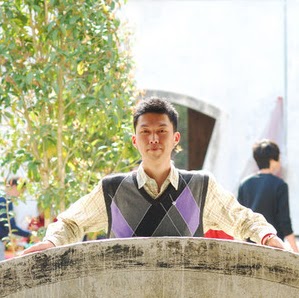
Yi Ma
Education:
Zhejiang University - Computer Science, Zhejiang University - Software Engineering

Yi Ma

Yi Ma

Yi Ma

Yi Ma

Yi Ma

Yi Ma

Yi Ma

Yi Ru Ma
view source
Yi Ma
view source
Qin Yi Ma
view source
Cheng Yi Ma
view source
Yi Ma
view source
Yi Ma
view source
Yi Shen Ma
view source
Yi Ma
view sourceFlickr
Youtube
Get Report for Yi Plan Ma from San Bruno, CA, age ~41


