Yu Jia Wang
age ~47
from San Jose, CA
- Also known as:
-
- Yu J Wang
- Jia Wang Yu
- Yujia Wang
- Yulan Wang
- Yushi Wang
- Yugia Wang
- Julie Pealer
- Julie Gonzales
Yu Wang Phones & Addresses
- San Jose, CA
- Palo Alto, CA
- Mountain View, CA
- Cupertino, CA
- Santa Clara, CA
- Chapel Hill, NC
- Mohegan Lake, NY
Us Patents
-
Method And Apparatus For Communicating In A Distributed Multiple Access Wireless Communication System
view source -
US Patent:6934297, Aug 23, 2005
-
Filed:Nov 2, 2000
-
Appl. No.:09/704807
-
Inventors:Brahim Bensaou - Kowloon, HK
Yu Wang - Santa Cruz CA, US -
Assignee:Agency for Science, Technology and Research - Singapore
-
International Classification:H04L012/413
-
US Classification:370445, 370348, 370443, 455450, 455451, 4554521
-
Abstract:A communication unit () that wants to transmit a data packet to another communication unit () must acquire access to a common communication channel (not shown) before transmitting a data packet (). For data packets of realtime applications, quality of service (QOS) parameters for the data packet are used to define transmission parameters to communicate the data packet (). These parameters include T() and T(). In addition, compliance with predetermined requirements of size relationship between request-to-send (RTS) and clear-to-send (CTS) packets are imposed.
-
Excessive Round-Hole Shielded Gate Trench (Sgt) Mosfet Devices And Manufacturing Processes
view source -
US Patent:7492005, Feb 17, 2009
-
Filed:Dec 28, 2005
-
Appl. No.:11/321957
-
Inventors:Hong Chang - Cupertino CA, US
Tiesheng Li - San Jose CA, US
Yu Wang - Fremont CA, US -
Assignee:Alpha & Omega Semiconductor, Ltd. - Hamilton
-
International Classification:H01L 29/76
-
US Classification:257330, 257340
-
Abstract:This invention discloses an improved trenched metal oxide semiconductor field effect transistor (MOSFET) device that includes a trenched gate surrounded by a source region encompassed in a body region above a drain region disposed on a bottom surface of a substrate. The MOSFET cell further includes a shielded gate trench (SGT) structure below and insulated from the trenched gate. The SGT structure is formed substantially as a round hole having a lateral expansion extended beyond the trench gate and covered by a dielectric liner layer filled with a trenched gate material. The round hole is formed by an isotropic etch at the bottom of the trenched gate and is insulated from the trenched gate by an oxide insulation layer. The round hole has a lateral expansion beyond the trench walls and the lateral expansion serves as a vertical alignment landmark for controlling the depth of the trenched gate. The MOSFET device has a reduced gate to drain capacitance Cgd depending on the controllable depth of the trenched gate disposed above the SGT structure formed as a round hole below the trenched gate.
-
Resistance-Based Etch Depth Determination For Sgt Technology
view source -
US Patent:7521332, Apr 21, 2009
-
Filed:Mar 23, 2007
-
Appl. No.:11/690581
-
Inventors:Tiesheng Li - San Jose CA, US
Yu Wang - Fremont CA, US
Yingying Lou - Shanghai, CN
Anup Bhalla - Santa Clara CA, US -
Assignee:Alpha & Omega Semiconductor, Ltd - Hamilton
-
International Classification:H01L 21/76
-
US Classification:438426
-
Abstract:A method for determining the depth etch, a method of forming a shielded gate trench (SGT) structure and a semiconductor device wafer are disclosed. A material layer is formed over part of a substrate having a trench. The material fills the trench. A resist mask is placed over a test portion of the material layer thereby defining a test structure that lies underneath the resist mask. The resist mask does not cover the trench. The material is isotropically etched and a signal related to a resistance change of the test structure is measured. A lateral undercut Dof the test structure is determined from the signal and an etch depth Dis determined from D. The wafer may comprise one or more test structures forming a bridge circuit; one or more metal contacts that electrically connect the test structures through contact holes: and resist layer including over the test structures.
-
Polysilicon Control Etch-Back Indicator
view source -
US Patent:7632733, Dec 15, 2009
-
Filed:Apr 29, 2006
-
Appl. No.:11/413248
-
Inventors:Yu Wang - Fremont CA, US
Tiesheng Li - San Jose CA, US
Hong Chang - Cupertino CA, US -
Assignee:Alpha & Omega Semiconductor, Inc. - Sunnyvale CA
-
International Classification:H01L 21/336
-
US Classification:438270, 257E2153
-
Abstract:This invention discloses a semiconductor wafer for manufacturing electronic circuit thereon. The semiconductor substrate further includes an etch-back indicator that includes trenches of different sizes having polysilicon filled in the trenches and then completely removed from some of the trenches of greater planar trench dimensions and the polysilicon still remaining in a bottom portion in some of the trenches having smaller planar trench dimensions.
-
Apparatus For Combinatorial Screening Of Electrochemical Materials
view source -
US Patent:7633267, Dec 15, 2009
-
Filed:Jul 5, 2005
-
Appl. No.:11/175555
-
Inventors:Keith Douglas Kepler - Belmont CA, US
Yu Wang - Foster City CA, US -
Assignee:Farasis Energy, Inc. - Hayward CA
-
International Classification:H01M 10/46
-
US Classification:320150
-
Abstract:A high throughput combinatorial screening method and apparatus for the evaluation of electrochemical materials using a single voltage source () is disclosed wherein temperature changes arising from the application of an electrical load to a cell array () are used to evaluate the relative electrochemical efficiency of the materials comprising the array. The apparatus may include an array of electrochemical cells () that are connected to each other in parallel or in series, an electronic load () for applying a voltage or current to the electrochemical cells (), and a device (), external to the cells, for monitoring the relative temperature of each cell when the load is applied.
-
Variable Volume Between Flexible Structure And Support Surface
view source -
US Patent:7710371, May 4, 2010
-
Filed:Dec 16, 2004
-
Appl. No.:11/014490
-
Inventors:Ping Mei - Palo Alto CA, US
Jurgen Daniel - Mountain View CA, US
James B. Boyce - Los Altos CA, US
Jackson Ho - Palo Alto CA, US
Rachel Lau - San Jose CA, US
Yu Wang - Union City CA, US -
Assignee:Xerox Corporation - Norwalk CT
-
International Classification:G09G 3/34
C25B 9/00
F04B 17/00
B41J 2/14
G02F 1/153
H04R 19/00 -
US Classification:345 85, 204253, 204255, 204257, 204252, 4174131, 347 49, 359267, 359291, 381176, 381399
-
Abstract:Cells can include variable volumes defined between a flexible structure, such as a polymer layer, and a support surface, with the flexible structure and support surface being attached in a first region that surrounds a second region in which they are unattached. Various adhesion structures can attach the flexible structure and the support surface. When unstretched, the flexible structure can lie in a flat position on the support surface. In response to a stretching force away from the support surface, the flexible structure can move out of the flat position, providing the variable volume. Electrodes, such as on the flexible structure, on the support surface, and over the flexible structure, can have charge levels that couple with each other and with the variable volume. A support structure can include a device layer with signal circuitry that provides a signal path between an electrode and external circuitry. One or more ducts can provide fluid communication with each cell's variable volume.
-
Resistance-Based Etch Depth Determination For Sgt Technology
view source -
US Patent:7795108, Sep 14, 2010
-
Filed:Mar 6, 2009
-
Appl. No.:12/399632
-
Inventors:Tiesheng Li - San Jose CA, US
Yu Wang - Fremont CA, US
Yingying Lou - Shanghai CA, US
Anup Bhalla - Santa Clara CA, US -
Assignee:Alpha & Omega Semiconductor, Ltd - Hamilton
-
International Classification:H01L 21/76
-
US Classification:438426
-
Abstract:A method for determining the depth etch, a method of forming a shielded gate trench (SGT) structure and a semiconductor device wafer are disclosed. A material layer is formed over part of a substrate having a trench. The material fills the trench. A resist mask is placed over a test portion of the material layer thereby defining a test structure that lies underneath the resist mask. The resist mask does not cover the trench. The material is isotropically etched and a signal related to a resistance change of the test structure is measured. A lateral undercut Dof the test structure is determined from the signal and an etch depth Dis determined from D. The wafer may comprise one or more test structures forming a bridge circuit; one or more metal contacts that electrically connect the test structures through contact holes: and resist layer including over the test structures.
-
Polysilicon Control Etch-Back Indicator
view source -
US Patent:7928507, Apr 19, 2011
-
Filed:Dec 9, 2009
-
Appl. No.:12/653130
-
Inventors:Yu Wang - Fremont CA, US
Tiesheng Li - San Jose CA, US
Hong Chang - Cupertino CA, US -
Assignee:Alpha & Omega Semiconductor, Inc. - Sunnyvale CA
-
International Classification:H01L 29/66
H01L 29/06 -
US Classification:257330, 257622, 257E2153, 257E21585
-
Abstract:This invention discloses a semiconductor wafer for manufacturing electronic circuit thereon. The semiconductor substrate further includes an etch-back indicator that includes trenches of different sizes having polysilicon filled in the trenches and then completely removed from some of the trenches of greater planar trench dimensions and the polysilicon still remaining in a bottom portion in some of the trenches having smaller planar trench dimensions.
Lawyers & Attorneys

Yu Wang - Lawyer
view sourceOffice:
Simpson Thacher & Bartlett LLP
Specialties:
Capital Markets and Securities
Corporate
Asia-Pacific Investment
Corporate
Asia-Pacific Investment
ISLN:
920534715
Admitted:
2008
University:
Boston University, Ph.D., 2005; Peking University, B.S., 1997
Law School:
The University of Michigan Law School, J.D., 2007
Medicine Doctors

Yu Wang
view sourceSpecialties:
Urology
Work:
Kaiser Permanente Medical GroupKaiser Permanente Fontana Medical Center
9961 Sierra Ave, Fontana, CA 92335
909 427-5000 (phone), 909 427-7366 (fax)
9961 Sierra Ave, Fontana, CA 92335
909 427-5000 (phone), 909 427-7366 (fax)
Education:
Medical School
Loma Linda University School of Medicine
Graduated: 1987
Loma Linda University School of Medicine
Graduated: 1987
Procedures:
Cystoscopy
Cystourethroscopy
Cystourethroscopy
Conditions:
Urinary Incontinence
Benign Prostatic Hypertrophy
Bladder Cancer
Calculus of the Urinary System
Erectile Dysfunction (ED)
Benign Prostatic Hypertrophy
Bladder Cancer
Calculus of the Urinary System
Erectile Dysfunction (ED)
Languages:
English
Description:
Dr. Wang graduated from the Loma Linda University School of Medicine in 1987. He works in Fontana, CA and specializes in Urology. Dr. Wang is affiliated with Kaiser Permanente Fontana Medical Center.

Yu Wang
view sourceSpecialties:
Urgent Care Medicine
Work:
US Healthworks
3223 1 Ave S STE C, Seattle, WA 98134
206 624-3651 (phone), 206 624-2391 (fax)
3223 1 Ave S STE C, Seattle, WA 98134
206 624-3651 (phone), 206 624-2391 (fax)
Languages:
Chinese
English
English
Description:
Dr. Wang works in Seattle, WA and specializes in Urgent Care Medicine.

Yu Cathy Wang
view sourceSpecialties:
Emergency Medicine
Education:
Oregon Health & Science University (2003)

Yu Kun Wang
view sourceSpecialties:
Family Medicine

Yu Richerd Wang
view sourceSpecialties:
Internal Medicine
Pulmonary Disease
Pulmonary Disease
Education:
Medical College Of Qingdao University (1988)
Wikipedia

Jimmy Wang (actor)
view sourceJimmy Wang Yu (Chinese: ; pinyin: Wng Y; Yale: Wong4 Jyu5; born March 28, 1943 in Wuxi, Jiangsu, also known as Wong Yu-lung and Wang Yue) is a Chinese ...
Isbn (Books And Publications)
-
The China Question: Essays On Current Relations Between Mainland China And Taiwan
view source -
Author:Yu San Wang
-
ISBN #:0275900460
-
Foreign Policy Of The Republic Of China On Taiwan: An Unorthodox Approach
view source -
Author:Yu S. Wang
-
ISBN #:0275934713
-
5Th Design For Manufacturing Conference
view source -
Author:Yu Michael Wang
-
ISBN #:0791835138
License Records
Yu Wang
License #:
3444 - Active
Category:
Massage Therapy
Issued Date:
Sep 14, 2016
Effective Date:
Sep 14, 2016
Expiration Date:
Nov 1, 2017
Type:
Massage Therapist
Name / Title
Company / Classification
Phones & Addresses
President
Future Byte Consulting, Inc
19925 Stevens Crk Blvd, Cupertino, CA 95014
President
Event Interactive, Inc
19925 Stevens Crk Blvd, Cupertino, CA 95014
President
U4LINKS, INC
Business Services at Non-Commercial Site
Business Services at Non-Commercial Site
1758 Beverly Blvd, San Jose, CA 95116
President
Farasis Energy, Inc.
Oil & Energy · Mfg Motors/Generators
Oil & Energy · Mfg Motors/Generators
21363 Cabot Blvd, Hayward, CA 94545
23575 Cabot Blvd, Hayward, CA 94545
510 732-6600
23575 Cabot Blvd, Hayward, CA 94545
510 732-6600
Principal
Consultant Harmony LLC Unison
Business Consulting Services
Business Consulting Services
325 Old Glory Ct, Fremont, CA 94539
Managing
Wit Expedient LLC
Marketing, Market Research, Product Loca
Marketing, Market Research, Product Loca
1255 W Washington Ave, Sunnyvale, CA 94086
Unison Harmony Consultant LLC
Consulting and Music · Musical Education
Consulting and Music · Musical Education
325 Old Glory Ct, Fremont, CA 94539
13751 Ln Paloma Rd, Los Altos, CA 94022
13751 Ln Paloma Rd, Los Altos, CA 94022
FU WANG INC
Resumes

Yu Wang Malden, MA
view sourceWork:
Apartment Property Management
Apr 2014 to Apr 2014 Virtual Inventory for Amazon One
Oct 2013 to Oct 2013 Mountain View Community Hospital
Mountain View, CA
Oct 2013 to Oct 2013 YiTianCheng Construction Engineering Design Co. Ltd
Nov 2011 to Nov 2011 Tianjin Zhongruan Dongli Co., Ltd
Jun 2011 to Jun 2011
Apr 2014 to Apr 2014 Virtual Inventory for Amazon One
Oct 2013 to Oct 2013 Mountain View Community Hospital
Mountain View, CA
Oct 2013 to Oct 2013 YiTianCheng Construction Engineering Design Co. Ltd
Nov 2011 to Nov 2011 Tianjin Zhongruan Dongli Co., Ltd
Jun 2011 to Jun 2011
Education:
Tianjin University of Finance & Economic
Jun 2012
Bachelor of Science in Network Engineering Northeastern University
Boston, MA
Master of Science in Information System
Jun 2012
Bachelor of Science in Network Engineering Northeastern University
Boston, MA
Master of Science in Information System

Yu Carolyn Wang
view source
Yu Tong Wang
view source
Yu Hsin Wang
view source
Yu Tsan Wang
view source
Yu Huai Wang
view source
Yu Hsin Wang
view source
Yu Long Wang
view source
Yu Christine Wang
view sourceYoutube
The Chinese Boxer Jimmy Wang Yu
The Chinese Boxer 1970 Jimmy Wang Yu, Lo Lieh, Wang Ping.
-
Category:Entertainment
-
Uploaded:22 Feb, 2009
-
Duration:3m 43s
14A (hui jia de yu wang episode 14 part A)
chinesehongkongs...
-
Category:Entertainment
-
Uploaded:19 Mar, 2011
-
Duration:15m
Myspace
Classmates

Yu Wang
view sourceSchools:
Dalian No. 8 High School Dalian China 1980-1984
Community:
Rocky Medina

Yu Wang
view sourceSchools:
Peking American High School Beijing China 1996-2000
Community:
Richard Capps

Yu Dong (Wang)
view sourceSchools:
Brumsted Elementary School Holland NY 1999-2003
Community:
Patrick Rietberg, Nego Jackson, John Smith, Arun Arun, Sadia Shamim, Aimee Prisinzano

Yu Hao Wang
view sourceSchools:
Ecole Secondaire Louis-Riel High School Montreal Kuwait 1998-2002
Community:
Vincent Weave, Mara Buruian, Kevin Girard, Krisztina Balogh, Yves Saindon, Simon Lamoureux, Julien Marsot, Antoine Pontbriand, Paul Goyer, Fernando Lafreniere

Yu Wang
view sourceSchools:
Laurentian University Sudbury Morocco 2002-2006
Community:
Debbie Mackay, Kimberley Andrus, Barbara Udal, Shelley Lineham

Yu Wang
view sourceSchools:
General Mortagne High School Boucherville Kuwait 1990-1994
Community:
Julie Christin, Eric Bergeron, Chantal Tremblay, Catherine Michaud, Michelle Atkinson, Nancy Hamelin, Isabel Rivard, Ben Rajotte

Peking American High Scho...
view sourceGraduates:
Yu Wang (1996-2000),
David Lin (1986-1990),
Waters Frank (1994-1998),
Green Bakus (2000-2003),
Patrick Baldwin (1983-1987),
Nick Wang (1986-1990)
David Lin (1986-1990),
Waters Frank (1994-1998),
Green Bakus (2000-2003),
Patrick Baldwin (1983-1987),
Nick Wang (1986-1990)

Pasadena Community Colleg...
view sourceGraduates:
Andrew Gallardo (2001-2005),
Fan Yu (2004-2008),
Tarissa Reese (2005-2006),
Jen Yu Wang (1994-1996),
Pohan Djingga (1984-1988)
Fan Yu (2004-2008),
Tarissa Reese (2005-2006),
Jen Yu Wang (1994-1996),
Pohan Djingga (1984-1988)
Plaxo

Wang Yu
view sourceKnming, Yunnan, ChinaPast: Center for Biodversity and Indigenous Knowledge

Wang Yu
view sourcePast: Engineering at Metallkraft Yangzhou, Engineer at ZPSS

Yu Wang
view sourceFlickr
Googleplus

Yu Wang
Work:
E.J.McKay - Business Analyst (2012)
Education:
Nanyang Technological University - Financial Engineering, Shanghai Jiao Tong University - Applied Physics

Yu Wang
Work:
GrapeCity - Global Architect Team (2008)
Education:
Fudan University - Information science and technology

Yu Wang
Work:
Uperform (2012)
ThoughtWorks (2007-2012)
ThoughtWorks (2007-2012)

Yu Wang
Education:
Michigan State University - Computer Science, Nanjing University - Electrical Engineering

Yu Wang
Work:
Dulukala - Officer (2011-2012)
Bragging Rights:
Work in Singapore>3

Yu Wang
Work:
Oracle Corporation - Enterprise Architecture
Education:
Huazhong University of Science and Technology - Ph.D. of Computer science, computer system architecture

Yu Wang
Education:
Polytech Tours - Informatique
Tagline:
.....
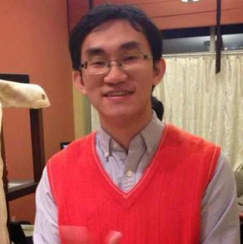
Yu Wang
Work:
New York University - Ph.D candidate
Education:
New York University
Get Report for Yu Jia Wang from San Jose, CA, age ~47


