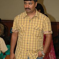
Srinivasa N Reddy
age ~47
from Bethesda, MD
- Also known as:
-
- Srinivasa S Reddy
- Sheshalatha R Reddy
- Srinvasa S Reddy
- Inivasa Reddy
- H Reddy
- Srinivas Reddy
- Vanamala Reddy
- Sn Reddy Srinivasa
- Reddy Srinivasa Sn
Srinivasa Reddy Phones & Addresses
- Bethesda, MD
- Silver Spring, MD
- Alexandria, VA
- Jersey City, NJ
- Lagrangeville, NY
- Chicago, IL
- Ann Arbor, MI
Wikipedia References

Srinivasa Reddy Srinivas Reddy
Work:
Position:
Telugu actor
Skills & Activities:
Activity:
Comedian
Medicine Doctors

Srinivasa A. Reddy
view sourceSpecialties:
Cardiovascular Disease
Work:
TexomaCareTexoma Heart Group
5026 Pool Rd, Denison, TX 75020
903 465-3624 (phone), 903 465-3973 (fax)
TexomaCareTexoma Heart Group
5026 Pool Rd, Denison, TX 75020
903 465-3624 (phone), 903 465-3973 (fax)
TexomaCareTexoma Heart Group
1727 Chuckwa Dr STE 400, Durant, OK 74701
580 924-7096 (phone), 903 465-3973 (fax)
5026 Pool Rd, Denison, TX 75020
903 465-3624 (phone), 903 465-3973 (fax)
TexomaCareTexoma Heart Group
5026 Pool Rd, Denison, TX 75020
903 465-3624 (phone), 903 465-3973 (fax)
TexomaCareTexoma Heart Group
1727 Chuckwa Dr STE 400, Durant, OK 74701
580 924-7096 (phone), 903 465-3973 (fax)
Procedures:
Angioplasty
Cardiac Catheterization
Cardiac Stress Test
Continuous EKG
Echocardiogram
Electrocardiogram (EKG or ECG)
Cardiac Catheterization
Cardiac Stress Test
Continuous EKG
Echocardiogram
Electrocardiogram (EKG or ECG)
Conditions:
Heart Failure
Ischemic Heart Disease
Acute Myocardial Infarction (AMI)
Angina Pectoris
Aortic Valvular Disease
Ischemic Heart Disease
Acute Myocardial Infarction (AMI)
Angina Pectoris
Aortic Valvular Disease
Languages:
English
Spanish
Spanish
Description:
Dr. Reddy works in Denison, TX and 2 other locations and specializes in Cardiovascular Disease. Dr. Reddy is affiliated with Texoma Medical Center.

Srinivasa H. Reddy
view sourceSpecialties:
Internal Medicine
Work:
Abrazo Health Arrowhead Hospital Hospitalists
18701 N 67 Ave, Glendale, AZ 85308
623 561-1000 (phone)
18701 N 67 Ave, Glendale, AZ 85308
623 561-1000 (phone)
Languages:
English
Description:
Dr. Reddy works in Glendale, AZ and specializes in Internal Medicine.

Srinivasa Donthi Reddy
view sourceLicense Records
Srinivasa Reddy
Phone:
352 326-0621 (Work)
License #:
33774 - Expired
Category:
Internal Medicine
Type:
Private Practice
Srinivasa R. Reddy
Phone:
270 886-4431 (Work)
License #:
34052 - Expired
Category:
Psychiatry
Type:
Hospital Based
Resumes

Srinivasa Reddy
view sourceWork:
Tesco Plc
Manager
Manager

Srinivasa Reddy
view sourceEducation:
Sri Sai Vikas Junior College 2009 - 2011
Bachelors, Bachelor of Technology, Mechanical Engineering
Bachelors, Bachelor of Technology, Mechanical Engineering

Srinivasa Reddy
view source
Srinivasa Reddy
view source
Srinivasa Reddy
view source
Srinivasa Reddy
view source
Srinivasa Reddy
view sourceLocation:
United States
Us Patents
-
Decoupling Capacitor Method And Structure Using Metal Based Carrier
view source -
US Patent:6461493, Oct 8, 2002
-
Filed:Dec 23, 1999
-
Appl. No.:09/472136
-
Inventors:Mukta S. Farooq - Hopewell Junction NY
Shaji Farooq - Hopewell Junction NY
John U. Knickerbocker - Hopewell Junction NY
Robert A. Rita - Wappingers Falls NY
Srinivasa N. Reddy - LaGrangeville NY -
Assignee:International Business Machines Corporation - Armonk NY
-
International Classification:C25D 502
-
US Classification:205118, 205122, 361311
-
Abstract:A process for fabricating a structure using a metal carrier and forming a double capacitor structure. The process comprises forming a first via hole through the metal carrier, forming a dielectric layer around the metal carrier and inside the first via hole, forming a second via hole through the dielectric layer and the metal carrier, and filling at least one of the via holes with conductive material. In one preferred embodiment, the process further comprises forming a third via hole through the metal carrier before the forming of a dielectric layer, wherein the dielectric layer is formed around the metal carrier, inside the first via hole, and inside the third via hole. The first via hole, the second via hole, and the third via hole are all filled with a conductive material. In one preferred embodiment, the dielectric layer comprises a top surface opposed to a bottom surface, and electrodes are formed on at least one of the top surface and the bottom surface of the dielectric layer.
-
Multi-Cavity Substrate Structure For Discrete Devices
view source -
US Patent:6489686, Dec 3, 2002
-
Filed:Mar 19, 2001
-
Appl. No.:09/812091
-
Inventors:Mukta S. Farooq - Hopewell Junction NY
John U. Knickerbocker - Hopewell Junction NY
Srinivasa S. Reddy - Lagrangeville NY -
Assignee:International Business Machines Corporation - Armonk NY
-
International Classification:H01L 2348
-
US Classification:257777, 257686, 257724
-
Abstract:The distance between a discrete or passive electrical component and an electrical semiconductor device and substrate or carrier is minimized by shortening the lead length connections of the passive component. One or more passive electronic components are mounted within the body of a carrier or board by creating a cavity in the substrate or carrier that is directly below a semiconductor device. The passive component is electrically connected to the substrate and device using solder bump technology resulting in much shorter lead length connections to and from the passive component.
-
Interposer Capacitor Built On Silicon Wafer And Joined To A Ceramic Substrate
view source -
US Patent:6791133, Sep 14, 2004
-
Filed:Jul 19, 2002
-
Appl. No.:10/200479
-
Inventors:Mukta Ghate Farooq - Hopewell Junction NY
John U. Knickerbocker - Hopewell Junction NY
Srinivasa Reddy - Lagrangeville NY
Robert Anthony Rita - Wappingers Falls NY -
Assignee:International Business Machines Corporation - Armonk NY
-
International Classification:H01L 23053
-
US Classification:257296, 536691, 536700
-
Abstract:An interposer, located between an integrated circuit having power, ground and signal connections and a ceramic substrate having power, ground and signal connections, that includes an oxide layer formed on a polished surface of a silicon substrate, a thin film dielectric capacitor formed on the oxide layer, a plurality of metallized that electrically connect to either of the electrodes of the thin film dielectric capacitor, and vias than conduct power, ground and signals between a the ceramic substrate and the integrated circuit. The interposer connects the metallized vias to the integrated circuit by solder connections and also connects the vias conducting power, ground and signals from the ceramic substrate to the interposer by solder connections. The dielectric of the thin film dielectric capacitor may be selected from the group of high-K titanates, such as, barium zirconate titanate, barium strontium titanate, pure barium titanate, barium titanate modified with Pb, Nb, W, Ca, Mg, and Zn, lead titanate, lead zirconate titanate, and polycrystalline lanthanum-modified lead zirconate titanate, or other high-K dielectrics, such as, lead niobate and its derivatives, and lead tungstate and its derivatives.
-
Enhanced High-Frequency Via Interconnection For Improved Reliability
view source -
US Patent:6900395, May 31, 2005
-
Filed:Nov 26, 2002
-
Appl. No.:10/306756
-
Inventors:Janet L. Jozwiak - Wappingers Falls NY, US
Gregory B. Martin - Wappingers Falls NY, US
Linda L. Rapp - Poughkeepsie NY, US
Srinivasa S. Reddy - Lagrangeville NY, US -
Assignee:International Business Machines Corporation - Armonk NY
-
International Classification:H05K001/11
H01R012/04 -
US Classification:174264, 174262, 174258, 361767, 257698
-
Abstract:Replacements of thick film pads with smaller, thinner, metal contacts or straps are used to eliminate many of the stress-related failure modes associated with the larger contact pads. These straps allow for a more simplified manufacturing process than that associated with an anchored I/O pad configuration. A single via, electrically connected to a plurality of vias in a substrate layer above, is introduced to enhance the reliability of the signal net, and provides for higher frequency applications through reduction in parasitic capacitance and electrical leakage. The straps are directionally located toward the substrate center. Once the locations of the internal strap vias are redirected to lower local distance-to-neutral points, still within the same I/O capture pad, and directed towards the center of the substrate, single vias are then placed at the strap end closest the substrate center.
-
Interposer Capacitor Built On Silicon Wafer And Joined To A Ceramic Substrate
view source -
US Patent:6943108, Sep 13, 2005
-
Filed:Jul 8, 2004
-
Appl. No.:10/885856
-
Inventors:Mukta Ghate Farooq - Hopewell Junction NY, US
John U. Knickerbocker - Hopewell Junction NY, US
Srinivasa Reddy - Lagrangeville NY, US
Robert Anthony Rita - Wappingers Falls NY, US -
Assignee:International Business Machines Corporation - Armonk NY
-
International Classification:H01L021/44
-
US Classification:438667, 361313, 361322, 361414, 438 10, 438 14, 438612
-
Abstract:An interposer, located between an integrated circuit having power, ground and signal connections and a ceramic substrate having power, ground and signal connections, that includes an oxide layer formed on a polished surface of a silicon substrate, a thin film dielectric capacitor formed on the oxide layer, a plurality of metallized that electrically connect to either of the electrodes of the thin film dielectric capacitor, and vias than conduct power, ground and signals between a the ceramic substrate and the integrated circuit. The interposer connects the metallized vias to the integrated circuit by solder connections and also connects the vias conducting power, ground and signals from the ceramic substrate to the interposer by solder connections. The dielectric of the thin film dielectric capacitor may be selected from the group of high-K titanates, such as, barium zirconate titanate, barium strontium titanate, pure barium titanate, barium titanate modified with Pb, Nb, W, Ca, Mg, and Zn, lead titanate, lead zirconate titanate, and polycrystalline lanthanum-modified lead zirconate titanate, or other high-K dielectrics, such as, lead niobate and its derivatives, and lead tungstate and its derivatives.
-
Multilayer Ceramic Substrate With Single Via Anchored Pad And Method Of Forming
view source -
US Patent:6987316, Jan 17, 2006
-
Filed:Jan 14, 2004
-
Appl. No.:10/707810
-
Inventors:Srinivasa N. Reddy - LaGrangeville NY, US
Mukta G. Farooq - Hopewell Junction NY, US
Kevin M. Prettyman - Poughkeepsie NY, US -
Assignee:International Business Machines Corporation - Armonk NY
-
International Classification:H01L 23/06
H01L 23/10
H01L 23/15 -
US Classification:257703, 257700, 257758
-
Abstract:A multilayer ceramic substrate in which an outer metal pad is anchored to the substrate by a single metal-filled via in the first ceramic layer adjacent to the metal pad. In turn, this single metal-filled via is anchored to the substrate by a larger, single metal-filled via in the next ceramic layer adjacent to the first ceramic layer. Preferably, the metal-filled vias and metal pad are 100 volume percent metal.
-
Discrete Magnets In Dielectric Forming Metal/Ceramic Laminate And Process Thereof
view source -
US Patent:20030205967, Nov 6, 2003
-
Filed:Jun 16, 2003
-
Appl. No.:10/462275
-
Inventors:Govindarajan Natarajan - Pleasant Valley NY, US
John Knickerbocker - Hopewell Junction NY, US
Srinivasa Reddy - LaGrangeville NY, US
Rao Vallabhaneni - Hopewell Junction NY, US -
International Classification:H01J001/62
-
US Classification:313/497000
-
Abstract:The present invention relates generally to a new dielectric forming metal/ceramic laminate magnet and process thereof. More particularly, the invention encompasses a new process for fabrication of a large area laminate magnet with a significant number of holes, integrated dielectric forming metal plate(s) and electrodes for electron and electron beam control. The present invention also relates to a magnetic matrix display and electron beam source and methods of manufacture thereof.
-
Method And Apparatus For Point Of Care Osmolarity Testing
view source -
US Patent:20070086927, Apr 19, 2007
-
Filed:Oct 14, 2005
-
Appl. No.:11/163327
-
Inventors:Govindarajan Natarajan - Poughkeepsie NY, US
James Humenik - LaGrangeville NY, US
Scott Partington - Raleigh NC, US
Srinivasa Reddy - LaGrangeville NY, US -
Assignee:INTERNATIONAL BUSINESS MACHINES CORPORATION - Armonk NY
-
International Classification:B01L 3/00
-
US Classification:422102000
-
Abstract:An apparatus and a method are disclosed for providing point of care testing for osmolarity of a bodily fluid. An apparatus is disclosed as having a fluid pathway passing through it for receiving and testing a sample fluid. The invention permits osmolarity testing of a sample fluid wherein the sample fluid has a volume of less than approximately 30 nL, and implements a method and device to measure fluid osmolarity in a clinical setting quickly and accurately, while also reducing evaporation of the fluid.
Classmates

Srinivasa Sridhar Reddy (...
view sourceSchools:
Good Shepherd School Miami FL 2002-2006
Community:
Walter Fisher, Albert Ray, Yader Gomez, Kristine Torres, Giselle Gomez, Good Good

Srinivasa Reddy
view sourceSchools:
University of North Carolina at Charlotte Charlotte NC 2000-2004
Community:
Candice Lalino, Fred Hoyle, Sara Gudi, Mohamed Honeine, Joe Ace, Laven Ramchandani, Robin Markham, Michelle Garrett, Manoj Akki, Andrew Hoover, Kay Hardy

Srinivasa Reddy Attipalli...
view source
Sri Vidya Vihar High Scho...
view sourceGraduates:
Srinivasa Reddy Putta (1978-1982),
Sharat Chandra (1995-1999)
Sharat Chandra (1995-1999)

University of North Carol...
view sourceGraduates:
Sudeshna Reddy Gunna (2003-2007),
Wilson Fletcher (1992-1996),
Srinivasa Reddy (2000-2004),
David Townsend (1972-1976)
Wilson Fletcher (1992-1996),
Srinivasa Reddy (2000-2004),
David Townsend (1972-1976)

West Jefferson High Schoo...
view sourceGraduates:
Srinivasa Reddy Bcom (2001-2005),
Landa Peeples (1979-1983),
April Elliott (1993-1997),
Selina Horton (1987-1991),
Patti Murphree (1988-1992)
Landa Peeples (1979-1983),
April Elliott (1993-1997),
Selina Horton (1987-1991),
Patti Murphree (1988-1992)
Flickr
Googleplus

Srinivasa Reddy
Work:
CMC Limited (2011)
IDS Soft (2004-2006)
Axsys healthtech (2006-2011)
IDS Soft (2004-2006)
Axsys healthtech (2006-2011)
Education:
Sri rama rural guruulam - SSC,Inter, SMIT,Chennai - B.Tech(I.T), SMUDE - MBA

Srinivasa Reddy
Work:
SRI CHAKRA CONSTRUCTIONS - Propreitor
Education:
Sri ramakrishna vidya peeta - High school, Vijaya pu college, jayanagar - Pre university, Sjcit, chikkaballapura - Bachelor of engineering civil, Manipal Institute of Technology - Mtech (Construction management)
Relationship:
Single
Tagline:
Never say never again

Srinivasa Reddy
Work:
Anglo-Eastern Group - Chief Engineer (2000)
Education:
APRS (Boys) Enkoor, Khammam Dist - 8th to 10th Class, Gowtam Junior College, Vijayawada - Intermediate, JNTU College of Engineering, Hyderabad - Engineering

Srinivasa Reddy
Work:
Nokia Siemens Networks - SE (2009)
Education:
National Institute of Technology Karnataka - MCA

Srinivasa Reddy
Work:
Juniper Networks
Education:
Masters

Srinivasa Reddy
Work:
IBM India
Education:
Kakathiya university

Srinivasa Reddy
Education:
Vignana bharati high school - S.s.c
Relationship:
Single
About:
I am srinivas & I hail from ongole. i'm persuing final b.tech in pridarshini college of engg.

Srinivasa Reddy
Work:
Land surveyor
Education:
Zp boys high school
Plaxo

Srinivasa Reddy
view source
Srinivasa Reddy kancherla
view sourceUttam Business Solutions
Myspace

Srinivasa Reddy Jakki Reddy
view source
M Srinivasa Reddy
view source
Srinivasa Reddy Satti
view source
Srinivasa Reddy Reddy
view source
Srinivasa Kalyan Reddy
view source
Srinivasa Reddy Reddy
view source
Srinivasa Reddy Reddy
view source
C B Srinivasa Reddy
view sourceYoutube
Get Report for Srinivasa N Reddy from Bethesda, MD, age ~47


