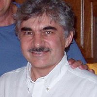
Scott H Holmberg
Deceased
from Escondido, CA
- Also known as:
-
- Scott Anna Trs Holmberg
- Scott H Holberg
- Michael Holmberg
- Phone and address:
-
3106 Las Palmas Ave, Escondido, CA 92025
760 233-0789
Scott Holmberg Phones & Addresses
- 3106 Las Palmas Ave, Escondido, CA 92025 • 760 233-0789
- Pleasanton, CA
- San Ramon, CA
- Commerce Township, MI
- San Diego, CA
- Livermore, CA
- Vallejo, CA
Medicine Doctors

Scott Dewey Holmberg
view sourceSpecialties:
Internal Medicine
Preventive Medicine
Public Health & General Preventive Medicine
General Preventive Medicine
Sports Medicine
Preventive Medicine
Public Health & General Preventive Medicine
General Preventive Medicine
Sports Medicine
Education:
Columbia University (1979)
Us Patents
-
Active Matrix Esd Protection And Testing Scheme
view source -
US Patent:6613650, Sep 2, 2003
-
Filed:May 10, 2000
-
Appl. No.:09/569111
-
Inventors:Scott H. Holmberg - Pleasanton CA
-
Assignee:Hyundai Electronics America - San Jose CA
-
International Classification:H01L 2100
-
US Classification:438438, 438 30, 349 38
-
Abstract:An improved method of manufacturing active matrix displays with ESD protection through final assembly and in process testing and repair capabilities. At least a first set of shorting bars is formed adjacent the row and column matrix. The shorting bars are respectively coupled to one another in series to allow testing of the matrix elements. A first shorting bar is coupled to the row lines and a second shorting bar is coupled to the column lines. The shorting bars can remain coupled to the matrix through final assembly to provide ESD protection and final assembly and testing capability.
-
Large Surface Area Dry Etcher
view source -
US Patent:20060042755, Mar 2, 2006
-
Filed:Aug 29, 2005
-
Appl. No.:11/215534
-
Inventors:Scott Holmberg - Escondido CA, US
Olivier Postel - Cupertino CA, US -
Assignee:PlasmaMed, LLC - Cupertino CA
-
International Classification:C23F 1/00
H01L 21/306 -
US Classification:156345100, 438706000, 216067000
-
Abstract:A dry etcher includes a process chamber configured to process a substrate therein using plasma; a substrate supporter to support the substrate; an inner chamber wall maintained at a high temperature and at least one magnetron provided in close proximity to the substrate to generate a local uniform high density plasma. The outer chamber wall provides vacuum integrity and is kept at low enough temperature to maintain vacuum integrity and to ensure safe operation of the machine. The dry etcher further includes a radio-frequency (RF) power source coupled to the substrate supporter, wherein the plasma is generated by the RF power applied to the substrate supporter and a magnetic field generated by the magnetron.
-
High Temperature Amorphous Memory Device For An Electrically Alterable Read-Only Memory
view source -
US Patent:41774752, Dec 4, 1979
-
Filed:Oct 31, 1977
-
Appl. No.:5/847068
-
Inventors:Scott H. Holmberg - Escondido CA
-
Assignee:Burroughs Corporation - Detroit MI
-
International Classification:H01L 4500
-
US Classification:357 2
-
Abstract:This disclosure relates to an electrically alterable amorphous memory device which can be switched from a high resistance state to a low resistance state, which device has a stable voltage threshold that is temperature insensitive throughout the lifetime of the device. The memory device is formed of a graded structure having at least three regions or layers of amorphous material selected from the tellurium based chalcogenide class of materials, particularly tellurium-germanium systems. The center or middle region is formed of the eutectic material which is in the range of 15 to 17 percent germanium although this range may vary from 10 to 25 percent. The top region or the region closest to the positive electrode is primarily tellurium with from 0 to 10 percent germanium. The bottom region or region closest to the negative electrode is formed of a material which has the highest glassy state transition temperature which material is approximately 33 percent germanium although this may vary from 25 to 45 percent germanium.
-
Method Of Manufacturing Thin Film Transistors And Transistors Made Thereby
view source -
US Patent:46511857, Mar 17, 1987
-
Filed:Apr 15, 1985
-
Appl. No.:6/723509
-
Inventors:Scott H. Holmberg - San Ramon CA
Richard A. Flasck - San Ramon CA -
Assignee:Alphasil, Inc. - Fremont CA
-
International Classification:H01L 2978
-
US Classification:357 237
-
Abstract:An improved method of manufacturing thin film transistors. A gate metal is patterned to form a gate electrode and a drain, gate and source contact pad for the transistor. To reduce shorts and capacitance between the gate and the source or the drain, a dielectric is patterned to form a central portion over a planar portion of the gate region and to cover any exposed gate edges.
-
Programmable Cell For Use In Programmable Electronic Arrays
view source -
US Patent:44995571, Feb 12, 1985
-
Filed:Jul 6, 1981
-
Appl. No.:6/281018
-
Inventors:Scott H. Holmberg - Milford MI
Richard A. Flasck - Rochester MI -
Assignee:Energy Conversion Devices, Inc. - Troy MI
-
International Classification:G11C 1300
-
US Classification:365163
-
Abstract:An improved programmable cell for use in programmable electronic arrays such as PROM devices, logic arrays, gate arrays and die interconnect arrays. The cells have a highly non-conductive state settable and non-resettable into a highly conductive state. The cells have a resistance of 10,000 ohms or more in the non-conductive state which are settable into the conductive state by a threshold voltage of 10 volts or less, a current of 25 milliamps or less, for 100 microseconds or less. The cells in the conductive state have a resistance of 100 ohms or less. The cells have a maximum permittable processing temperature of 400. degree. centigrade or more and a storage temperature of 175. degree. centigrade or more. The cells are formed from doped silicon alloys including at least hydrogen and/or fluorine and contain from about 0.
-
Active Matrix Esd Protection And Testing Scheme
view source -
US Patent:56680325, Sep 16, 1997
-
Filed:Jul 31, 1995
-
Appl. No.:8/497372
-
Inventors:Scott H. Holmberg - Pleasanton CA
Quy Vu - Fremont CA -
International Classification:H01L 21786
G02F 11343 -
US Classification:438144
-
Abstract:An improved method of manufacturing active matrix displays with ESD protection through final assembly and in process testing and repair capabilities. At least a first set of shorting bars is formed adjacent the row and column matrix. The shorting bars are respectively coupled to one another in series to allow testing of the matrix elements. A first shorting bar is coupled to the odd row lines, a second shorting bar is coupled to the even row lines, a third shorting bar is coupled to the odd column lines and a fourth shorting bar is coupled to the even column lines. The shorting bars can remain coupled to the matrix through final assembly to provide ESD protection and final assembly and testing capability.
-
Method Of Manufacturing Flat Panel Backplanes Including Redundant Gate Lines And Displays Made Thereby
view source -
US Patent:51629313, Nov 10, 1992
-
Filed:Nov 6, 1990
-
Appl. No.:7/609576
-
Inventors:Scott H. Holmberg - Pleasanton CA
-
Assignee:Honeywell, Inc. - Minneapolis MN
-
International Classification:G02F 113
-
US Classification:359 54
-
Abstract:Flat panel displays are provided with overlying interconnected and hence redundant bus lines to reduce fatal defects. The redundant, generally row lines are interconnected at least at two locations on a line and can be connected at each pixel to further reduce defects. The redundant row or gate line is formed by an overlying light shield line which preferably is of low resistivity and enhances the operation of the displays. The display can include subdivided subpixels and one defective subpixel is generally an acceptable non-fatal display defect, since the rest of the subpixels are still operative. The subpixels can be formed with common or redundant column bus lines.
-
Method Of Manufacturing Flat Panel Backplanes Including Electrostatic Discharge Prevention And Displays Made Thereby
view source -
US Patent:50190024, May 28, 1991
-
Filed:Jul 12, 1989
-
Appl. No.:7/218312
-
Inventors:Scott H. Holmberg - San Ramon CA
-
Assignee:Honeywell, Inc. - Minneapolis MN
-
International Classification:H01L 4500
-
US Classification:445 24
-
Abstract:Flat panel displays are provided including protection from electrostatic discharge (ESD) during manufacture and thereafter. At least one ESD guard ring is provided to protect the active elements of the display from the potential discharge between the row and column lines. An internal ESD guard ring is coupled to the row and column lines via shunt transistors. An external ESD guard ring is coupled to the row and column lines via a resistance. Both of the guard rings can be provided; however, the external guard ring is removed prior to completion of the display.
Name / Title
Company / Classification
Phones & Addresses
President, Owner
DONCON, INC
Filling Stations Gas · General Auto Repair · Auto Repair
Filling Stations Gas · General Auto Repair · Auto Repair
7731 Balboa Ave, San Diego, CA 92111
8110 Balboa Ave, San Diego, CA 92111
858 279-1010, 858 571-9784
8110 Balboa Ave, San Diego, CA 92111
858 279-1010, 858 571-9784
President
LIGHTSMITH, INC
Whol Durable Goods
Whol Durable Goods
3106 Las Palmas Ave, Escondido, CA 92025
Resumes

Pr. Systems Engineer At Rockwell Collins
view sourcePosition:
Pr. Systems Engineer at Rockwell Collins
Location:
Cedar Rapids, Iowa
Industry:
Aviation & Aerospace
Work:
Rockwell Collins - Cedar Rapids, Iowa Area since Jan 2013
Pr. Systems Engineer
Pr. Systems Engineer
Education:
Stevens Institute of Technology 2011 - 2012
Graduate Certificate, Systems Engineering and Architecting North Dakota State University 1991 - 1995
BS, Electrical Engineering
Graduate Certificate, Systems Engineering and Architecting North Dakota State University 1991 - 1995
BS, Electrical Engineering

Computer Software Professional
view sourceLocation:
Temecula, California
Industry:
Computer Networking
Work:
Volt / Aerotek - Tempe, AZ Jul 2012 - Feb 2013
Tier I Technical Support
Newport Mesa Unified School District Jan 2003 - Jan 2008
Teachers Assistant
City of Costa Mesa Jan 2001 - Jan 2003
After School Program Leader
Tier I Technical Support
Newport Mesa Unified School District Jan 2003 - Jan 2008
Teachers Assistant
City of Costa Mesa Jan 2001 - Jan 2003
After School Program Leader
Education:
Computer Training Academy 2010 - 2012
Certifications, Computer/Information Technology Administration and Management California State University-Long Beach 2006 - 2008
+40 Units, Liberal Arts and Sciences/Liberal Studies Orange Coast College 1988 - 2003
Transferred to CSULB with General Education, Liberal Arts and Sciences/Liberal Studies
Skills:
Microsoft Windows 98
Windows Server 2003
Windows 7
Windows XP Professional
Virtualization
Desktop Support
Network Administration
Network Infrastructure
VPN
Windows Server 2008
Disaster Recovery
DNS management
RAID
Router Configuration
Active Directory
Firewalls
Computer Hardware
Backup Solutions
Wiring/Cabling
TCP/IP
IPX/SPX
NAT
RIP
IGRP
PPP
L2TP
WINS
DHCP Management
WSUS
HTTP
HTTPS
FTP
Ethernet
Point to Point
ISDN
Twisted Pair
Fiber Optics
Coax
Serial Communications
Wireless Networking
Switches
Bridges
Hubs
Wireless Access Points
Printers

Owner, Holmberg Automotive
view sourcePosition:
Owner at HOLMBERG AUTOMOTIVE
Location:
Greater San Diego Area
Industry:
Automotive
Work:
HOLMBERG AUTOMOTIVE
Owner
Owner

Scott Holmberg
view sourceLocation:
United States
Classmates

Scott Holmberg
view sourceSchools:
Queen of Peace School Buffalo NY 1980-1983, Queen of Martyrs School Cheektowaga NY 1983-1987, Our Lady Help of Christians School Cheektowaga NY 1987-1990
Community:
Ronald Kwiatkowski

Scott Holmberg, Buhler Hi...
view source
Our Lady Help of Christia...
view sourceGraduates:
Scott Holmberg (1987-1990),
Mary Lane (1962-1970),
Colleen Zimmerman (1973-1982),
Daniel Coleman (1965-1973)
Mary Lane (1962-1970),
Colleen Zimmerman (1973-1982),
Daniel Coleman (1965-1973)

Sahuaro High School, Tucs...
view sourceGraduates:
Scott Holmberg (1977-1981),
Sara Fischer (1993-1997),
William Reid (1983-1987),
Michael Villafane (1977-1981),
Randy Boykin (1974-1978)
Sara Fischer (1993-1997),
William Reid (1983-1987),
Michael Villafane (1977-1981),
Randy Boykin (1974-1978)
Googleplus

Scott Holmberg

Scott Holmberg
Youtube

Scott Holmberg
view source
Scott Holmberg
view source
Scott Holmberg
view source
Scott Holmberg
view source
Scott Holmberg
view source
Scott Dewey Holmberg
view source
Scott Holmberg
view source
Scott Holmberg
view sourceMyspace
News

Miriam Hospital physician advocates awareness, collaboration to combat ...
view source- featuring the installation of 80 bonfires floating on Providence's three rivers, is part of the first free, evening artistic summer HCV festival to help bring awareness to the disease. Scott Holmberg, MD, MPH, Chief of Epidemiology and Surveillance for Viral Hepatitis at the CDC, will be the guest of honor.
- Date: Jul 24, 2014
- Category: Health
- Source: Google

Hepatitis C Now Kills More Americans Than HIV
view source- SOURCES: Scott Holmberg, M.D., M.P.H., chief, epidemiology and surveillance branch, division of viral hepatitis, U.S. Centers for Disease Control and Prevention; Eugene R. Schiff, M.D., Leonard Miller Professor of Medicine, director, Schiff Liver Institute/Center for Liver Diseases, University of Mi
- Date: Feb 21, 2012
- Category: Health
- Source: Google

Hepatitis C Now Kills More Americans Than HIV
view source- "These data underscore the urgent need to address the health threat posed by chronic hepatitis B and C in the United States," said investigator Dr. Scott Holmberg, chief of the Epidemiology and Surveillance Branch in CDC's Division of Viral Hepatitis.
- Date: Feb 21, 2012
- Category: Health
- Source: Google
Get Report for Scott H Holmberg from Escondido, CADeceased


