Amit J Bansal
age ~50
from Jericho, NY
- Also known as:
-
- Amit A Bansal
- Amit Barisal
- Amit B Ansal
- Ashish Bansal
- Amit Bansak
- Amit Vansal
Amit Bansal Phones & Addresses
- Jericho, NY
- 1044 Everglades Dr, Allen, TX 75013
- Dallas, TX
- 405 Rancho Arroyo Pkwy, Fremont, CA 94536 • 510 713-8781 • 510 742-1105
- 34313 Portia Ter, Fremont, CA 94555 • 510 713-8781
- 1129 Meadow Creek Dr, Irving, TX 75038 • 972 550-9160
- Fitchburg, WI
Work
-
Company:Ambulatory Care Center RUSK Rehabilitation
-
Address:240 E 38Th St, New York, NY 10016
-
Phones:212 263-6037 212 263-0418
Education
-
School / High School:New York College Of Osteopathic Medicine2005
Languages
English • Hindi
Awards
Healthgrades Honor Roll • NYU 2012 Teacher of The Year, June 2012
Ranks
-
Certificate:Internal Medicine, 2009
Images
Specialities
Internal Medicine • Physical Medicine & Rehabilitation
Medicine Doctors
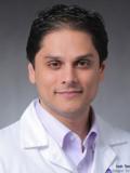
Dr. Amit K Bansal, New York NY - DO (Doctor of Osteopathic Medicine)
view sourceSpecialties:
Internal Medicine
Physical Medicine & Rehabilitation
Physical Medicine & Rehabilitation
Age:
46
Address:
Ambulatory Care Center RUSK Rehabilitation
240 E 38Th St, New York, NY 10016
212 263-6037 (Phone), 212 263-0418 (Fax)
240 E 38Th St, New York, NY 10016
212 263-6037 (Phone), 212 263-0418 (Fax)
Procedures:
Injection Therapy
Knee Problems
Neck Disorders
Knee Problems
Neck Disorders
Conditions:
Amputees
Back Pain
Hip Arthritis
Knee Osteoarthritis
Knee Problems and Injuries
Back Pain
Hip Arthritis
Knee Osteoarthritis
Knee Problems and Injuries
Certifications:
Internal Medicine, 2009
Awards:
Healthgrades Honor Roll
NYU 2012 Teacher of The Year, June 2012
NYU 2012 Teacher of The Year, June 2012
Languages:
English
Hindi
Hindi
Hospitals:
Ambulatory Care Center RUSK Rehabilitation
240 E 38Th St, New York, NY 10016
NYU Langone Medical Center
550 1St Avenue, New York, NY 10016
240 E 38Th St, New York, NY 10016
NYU Langone Medical Center
550 1St Avenue, New York, NY 10016
Philosophy:
To treat each patient as an individual with a quality of care far exceeding most standards. Improve communication between provider and patient so that we may come out with the best possible outcome using the newest agents to treat conditions
Education:
Medical School
New York College Of Osteopathic Medicine
Graduated: 2005
Medical School
Northshore Lij Hospital
Graduated: 2006
Medical School
Nyu Langone-Rusk Rehabilitation Institute
Graduated: 2009
Medical School
New York Institute Of Technology
Graduated: 2000
New York College Of Osteopathic Medicine
Graduated: 2005
Medical School
Northshore Lij Hospital
Graduated: 2006
Medical School
Nyu Langone-Rusk Rehabilitation Institute
Graduated: 2009
Medical School
New York Institute Of Technology
Graduated: 2000

Amit K. Bansal
view sourceSpecialties:
Obstetrics & Gynecology
Work:
Amit Bansal MD
4102 Woodlawn Ave STE 260, Pasadena, TX 77504
713 944-0076 (phone), 713 944-0283 (fax)
4102 Woodlawn Ave STE 260, Pasadena, TX 77504
713 944-0076 (phone), 713 944-0283 (fax)
Education:
Medical School
University of Texas Southwestern Medical Center at Dallas
Graduated: 1986
University of Texas Southwestern Medical Center at Dallas
Graduated: 1986
Procedures:
Hysterectomy
Skin Tags Removal
Skin Tags Removal
Conditions:
Abnormal Vaginal Bleeding
Breast Disorders
Genital HPV
Uncomplicated or Low Risk Pregnancy and Delivery
Candidiasis of Vulva and Vagina
Breast Disorders
Genital HPV
Uncomplicated or Low Risk Pregnancy and Delivery
Candidiasis of Vulva and Vagina
Languages:
English
Spanish
Spanish
Description:
Dr. Bansal graduated from the University of Texas Southwestern Medical Center at Dallas in 1986. He works in Pasadena, TX and specializes in Obstetrics & Gynecology. Dr. Bansal is affiliated with Bayshore Medical Center and Memorial Hermann Southeast Hospital.

Amit Bansal
view sourceSpecialties:
Internal Medicine
Work:
Rochester General Hospital Hospitalists
1425 Portland Ave STE 287, Rochester, NY 14621
585 922-5067 (phone), 585 922-2908 (fax)
1425 Portland Ave STE 287, Rochester, NY 14621
585 922-5067 (phone), 585 922-2908 (fax)
Education:
Medical School
Univ Coll of Med Sciences, Delhi Univ, New Delhi, Delhi, India
Graduated: 2002
Univ Coll of Med Sciences, Delhi Univ, New Delhi, Delhi, India
Graduated: 2002
Languages:
English
Description:
Dr. Bansal graduated from the Univ Coll of Med Sciences, Delhi Univ, New Delhi, Delhi, India in 2002. He works in Rochester, NY and specializes in Internal Medicine. Dr. Bansal is affiliated with Newark-Wayne Community Hospital.

Amit Bansal
view sourceSpecialties:
Internal Medicine
Work:
Boonshoft Internal Medicine Residency Program
128 E Apple St FL 2, Dayton, OH 45409
937 208-2866 (phone), 937 208-5304 (fax)
128 E Apple St FL 2, Dayton, OH 45409
937 208-2866 (phone), 937 208-5304 (fax)
Languages:
English
Description:
Dr. Bansal works in Dayton, OH and specializes in Internal Medicine. Dr. Bansal is affiliated with Miami Valley Hospital.

Amit Bansal
view sourceSpecialties:
Internal Medicine

Amit K Bansal, New York NY
view sourceSpecialties:
Physiatrist
Address:
301 E 17Th St, New York, NY 10003
550 1St Ave, New York, NY 10016
550 1St Ave, New York, NY 10016
Amazon

Innovative Processing and Synthesis of Ceramics, Glasses, and Composites V: Proceedings of the symposium held at the 103rd Annual Meeting of The ... Volume 129 (Ceramic Transactions Series)
view sourceThe most recent advancements in the areas of ceramic/composite processing and characterization are presented in this new volume. Selected topics include sol-gel processing, microwave sintering, reaction forming/bonding, polymer precursors, rapid prototyping, mechanical alloying, diamond and diamond-...
Binding
Hardcover
Pages
220
Publisher
Wiley-American Ceramic Society
ISBN #
1574981374
EAN Code
9781574981377
ISBN #
3

World Insolvency Systems: A Comparative Study
view sourceAuthor
Otto Eduardo Fonseca Lobo
Binding
Paperback
Pages
835
Publisher
Carswell Legal Pubns
ISBN #
0779821300
EAN Code
9780779821303
ISBN #
1
Us Patents
-
Tunable Ground Planes In Plasma Chambers
view source -
US Patent:20090236214, Sep 24, 2009
-
Filed:Mar 20, 2008
-
Appl. No.:12/052431
-
Inventors:Karthik Janakiraman - San Jose CA, US
Thomas Nowak - Cupertino CA, US
Juan Carlos Rocha-Alvarez - San Carlos CA, US
Mark A. Fodor - Los Gatos CA, US
Dale R. Du Bois - Los Gatos CA, US
Amit Bansal - Santa Clara CA, US
Mohamad Ayoub - San Jose CA, US
Eller Y. Juco - San Jose CA, US
Visweswaren Sivaramakrishnan - Cupertino CA, US
Hichem M'Saad - Santa Clara CA, US -
International Classification:C23C 16/00
H05H 1/24 -
US Classification:204164, 118723 R
-
Abstract:An apparatus and method are provided for controlling the intensity and distribution of a plasma discharge in a plasma chamber. In one embodiment, a shaped electrode is embedded in a substrate support to provide an electric field with radial and axial components inside the chamber. In another embodiment, the face plate electrode of the showerhead assembly is divided into zones by isolators, enabling different voltages to be applied to the different zones. Additionally, one or more electrodes may be embedded in the chamber side walls.
-
Apparatus And Method For Substrate Clamping In A Plasma Chamber
view source -
US Patent:20110090613, Apr 21, 2011
-
Filed:Nov 19, 2010
-
Appl. No.:12/950105
-
Inventors:Ganesh Balasubramanian - Sunnyvale CA, US
Amit Bansal - Santa Clara CA, US
Eller Y. Juco - San Jose CA, US
Mohamad Ayoub - San Jose CA, US
Hyung-Joon Kim - Sunnyvale CA, US
Karthik Janakiraman - San Jose CA, US
Sudha Rathi - San Jose CA, US
Deenesh Padhi - Sunnyvale CA, US
Martin Jay Seamons - San Jose CA, US
Visweswaren Sivaramakrishnan - Cupertino CA, US
Bok Hoen Kim - San Jose CA, US
Amir Al-Bayati - San Jose CA, US
Derek R. Witty - Fremont CA, US
Hichem M'Saad - Santa Clara CA, US
Anton Baryshnikov - San Jose CA, US
Chiu Chan - Foster City CA, US
Shuang Liu - Saratoga CA, US -
International Classification:H01L 21/683
H01L 21/66
G01R 27/02 -
US Classification:361234, 438 17, 702 65
-
Abstract:The present invention generally provides methods and apparatus for monitoring and maintaining flatness of a substrate in a plasma reactor. Certain embodiments of the present invention provide a method for processing a substrate comprising positioning the substrate on an electrostatic chuck, applying an RF power between the an electrode in the electrostatic chuck and a counter electrode positioned parallel to the electrostatic chuck, applying a DC bias to the electrode in the electrostatic chuck to clamp the substrate on the electrostatic chuck, and measuring an imaginary impedance of the electrostatic chuck.
-
Shadow Ring For Modifying Wafer Edge And Bevel Deposition
view source -
US Patent:20110159211, Jun 30, 2011
-
Filed:Dec 21, 2010
-
Appl. No.:12/974365
-
Inventors:Dale R. Du Bois - Los Gatos CA, US
Mohamad A. Ayoub - Las Gatos CA, US
Robert Kim - Mountain View CA, US
Amit Bansal - Santa Clara CA, US
Mark Fodor - Los Gatos CA, US
Binh Nguyen - San Jose CA, US
Siu F. Cheng - Los Angeles CA, US
Hang Yu - Woodland CA, US
Chiu Chan - Foster City CA, US
Ganesh Balasubramanian - Sunnyvale CA, US
Deenesh Padhi - Sunnyvale CA, US
Juan Carlos Rocha - San Carlos CA, US -
Assignee:APPLIED MATERIALS, INC. - Santa Clara CA
-
International Classification:C23C 16/00
B05C 11/00 -
US Classification:427569, 118 71
-
Abstract:Embodiments of the invention contemplate a shadow ring that provides increased or decreased and more uniform deposition on the edge of a wafer. By removing material from the top and/or bottom surfaces of the shadow ring, increased edge deposition and bevel coverage can be realized. In one embodiment, the material on the bottom surface is reduced by providing a recessed slot on the bottom surface. By increasing the amount of material of the shadow ring, the edge deposition and bevel coverage is reduced. Another approach to adjusting the deposition at the edge of the wafer includes increasing or decreasing the inner diameter of the shadow ring. The material forming the shadow ring may also be varied to change the amount of deposition at the edge of the wafer.
-
Confined Process Volume Pecvd Chamber
view source -
US Patent:20110294303, Dec 1, 2011
-
Filed:May 6, 2011
-
Appl. No.:13/102846
-
Inventors:Ramprakash Sankarakrishnan - San Jose CA, US
Ganesh Balasubramanian - Sunnyvale CA, US
Juan Carlos Rocha-Alvarez - San Carlos CA, US
Dale R. Du Bois - Los Gatos CA, US
Mark Fodor - Los Gatos CA, US
Jianhua Zhou - San Jose CA, US
Amit Bansal - Sunnyvale CA, US
Mohamad A. Ayoub - Las Gatos CA, US
Shahid Shaikh - Santa Clara CA, US
Patrick Reilly - Dublin CA, US
Deenesh Padhi - Sunnyvale CA, US
Thomas Nowak - Cupertino CA, US -
Assignee:APPLIED MATERIALS, INC. - Santa Clara CA
-
International Classification:C23C 16/44
H01L 21/30
C23C 16/509 -
US Classification:438758, 118723 E, 118504, 257E21211
-
Abstract:An apparatus for plasma processing a substrate is provided. The apparatus comprises a processing chamber, a substrate support disposed in the processing chamber, a shield member disposed in the processing chamber below the substrate support, and a lid assembly coupled to the processing chamber. The lid assembly comprises a conductive gas distributor coupled to a power source, and an electrode separated from the conductive gas distributor and the chamber body by electrical insulators. The electrode is also coupled to a source of electric power. The substrate support is formed with a stiffness that permits very little departure from parallelism. The shield member thermally shields a substrate transfer opening in the lower portion of the chamber body. A pumping plenum is located below the substrate support processing position, and is spaced apart therefrom.
-
Tunable Ground Planes In Plasma Chambers
view source -
US Patent:20120205046, Aug 16, 2012
-
Filed:Apr 26, 2012
-
Appl. No.:13/456308
-
Inventors:Karthik Janakiraman - San Jose CA, US
Thomas Nowak - Cupertino CA, US
Juan Carlos Rocha-Alvarez - San Carlos CA, US
Mark A. Fodor - Los Gatos CA, US
Dale R. Du Bois - Los Gatos CA, US
Amit Bansal - Sunnyvale CA, US
Mohamad A. Ayoub - Los Gatos CA, US
Eller Y. Juco - San Jose CA, US
Visweswaren Sivaramakrishnan - Cupertino CA, US
Hichem M'Saad - Santa Clara CA, US -
Assignee:APPLIED MATERIALS, INC. - Santa Clara CA
-
International Classification:H01L 21/3065
-
US Classification:15634534
-
Abstract:An apparatus and method are provided for controlling the intensity and distribution of a plasma discharge in a plasma chamber. In one embodiment, a shaped electrode is embedded in a substrate support to provide an electric field with radial and axial components inside the chamber. In another embodiment, the face plate electrode of the showerhead assembly is divided into zones by isolators, enabling different voltages to be applied to the different zones. Additionally, one or more electrodes may be embedded in the chamber side walls.
-
Apparatus And Method For Uv Treatment, Chemical Treatment, And Deposition
view source -
US Patent:20120258259, Oct 11, 2012
-
Filed:Apr 5, 2012
-
Appl. No.:13/440720
-
Inventors:Amit Bansal - Sunnyvale CA, US
Dale R. Du Bois - Los Gatos CA, US
Juan Carlos Rocha-Alvarez - San Carlos CA, US
Sanjeev Baluja - Campbell CA, US
Scott A. Hendrickson - Brentwood CA, US
Thomas Nowak - Cupertino CA, US -
International Classification:C23C 16/455
C23C 16/46
C23C 16/458 -
US Classification:427558, 118723 R, 118719
-
Abstract:Embodiments of the present invention provide apparatus and methods for performing UV treatment and chemical treatment and/or deposition in the same chamber. One embodiment of the present invention provides a processing chamber including a UV transparent gas distribution showerhead disposed above a substrate support located in an inner volume of the processing chamber, a UV transparent window disposed above the UV transparent gas distribution showerhead, and a UV unit disposed outside the inner volume. The UV unit is configured to direct UV lights towards the substrate support through the UV transparent window and the UV transparent gas distribution showerhead.
-
Apparatus And Method For Substrate Clamping In A Plasma Chamber
view source -
US Patent:20080084650, Apr 10, 2008
-
Filed:Oct 3, 2007
-
Appl. No.:11/866646
-
Inventors:Ganesh Balasubramanian - Sunnyvale CA, US
Amit Bansal - Santa Clara CA, US
Eller Juco - San Jose CA, US
Mohamad Ayoub - San Jose CA, US
Hyung-Joon Kim - Sunnyvale CA, US
Karthik Janakiraman - San Jose CA, US
Sudha Rathi - San Jose CA, US
Deenesh Padhi - Sunnyvale CA, US
Martin Seamons - San Jose CA, US
Visweswaren Sivaramakrishnan - Cupertino CA, US
Bok Kim - San Jose CA, US
Amir Al-Bayati - San Jose CA, US
Derek Witty - Fremont CA, US
Hichem M'Saad - Santa Clara CA, US
Anton Baryshnikov - San Jose CA, US
Chiu Chan - Foster City CA, US
Shuang Liu - Saratoga CA, US -
International Classification:H01L 21/683
-
US Classification:361234000
-
Abstract:The present invention generally provides methods and apparatus for monitoring and maintaining flatness of a substrate in a plasma reactor. Certain embodiments of the present invention provide a method for processing a substrate comprising positioning the substrate on an electrostatic chuck, applying an RF power between the an electrode in the electrostatic chuck and a counter electrode positioned parallel to the electrostatic chuck, applying a DC bias to the electrode in the electrostatic chuck to clamp the substrate on the electrostatic chuck, and measuring an imaginary impedance of the electrostatic chuck.
-
Treatment For High-Temperature Cleans
view source -
US Patent:20220384161, Dec 1, 2022
-
Filed:May 25, 2021
-
Appl. No.:17/330061
-
Inventors:- Santa Clara CA, US
Ruiyun Huang - Santa Clara CA, US
Abdul Aziz Khaja - San Jose CA, US
Amit Bansal - Milpitas CA, US
Dong Hyung Lee - Danville CA, US
Ganesh Balasubramanian - Fremont CA, US
Tuan Anh Nguyen - San Jose CA, US
Sungwon Ha - Palo Alto CA, US
Anjana M. Patel - San Jose CA, US
Ratsamee Limdulpaiboon - San Jose CA, US
Karthik Janakiraman - San Jose CA, US
Kwangduk Douglas Lee - Redwood City CA, US -
Assignee:Applied Materials, Inc. - Santa Clara CA
-
International Classification:H01J 37/32
B08B 7/00
C23C 14/56 -
Abstract:Exemplary methods of treating a chamber may include delivering a cleaning precursor to a remote plasma unit. The methods may include forming a plasma of the cleaning precursor. The methods may include delivering plasma effluents of the cleaning precursor to a processing region of a semiconductor processing chamber. The processing region may be defined by one or more chamber components. The one or more chamber components may include an oxide coating. The methods may include halting delivery of the plasma effluents. The methods may include treating the oxide coating with a hydrogen-containing material delivered to the processing region subsequent halting delivery of the plasma effluents.
Name / Title
Company / Classification
Phones & Addresses
President
AB COMPUTING SYSTEMS, INC
Employment Agency Custom Computer Programing
Employment Agency Custom Computer Programing
1900 Wyatt Dr, Santa Clara, CA 95054
5976 W Las Positas Blvd, Pleasanton, CA 94588
5658 Owens Dr, Pleasanton, CA 94588
5976 W Las Positas Blvd, Pleasanton, CA 94588
5658 Owens Dr, Pleasanton, CA 94588
CFO
Axygen
Biotechnology · Laboratory Equipment & Supplie · All Other Plastics Product Manufacturing
Biotechnology · Laboratory Equipment & Supplie · All Other Plastics Product Manufacturing
33210 Central Ave, Union City, CA 94587
33170 Central Ave, Union City, CA 94587
510 494-8900, 510 494-0700, 510 494-8900
33170 Central Ave, Union City, CA 94587
510 494-8900, 510 494-0700, 510 494-8900
Physical Medicine
Wallace Lehman
Medical Doctor's Office
Medical Doctor's Office
301 E 17 St, New York, NY 10003
212 598-6403
212 598-6403
AGS HOTEL, INC
A B S HOTELS INC
AS HOTELS INC
Amit Bansal MD,DO
Physical Medicine
Physical Medicine
301 E 17 St, New York, NY 10003
212 598-6267
212 598-6267
President, Chief Executive Officer
Sg Industries Inc
Whol Women's/Child's Clothing Whol Men's/Boy's Clothing
Whol Women's/Child's Clothing Whol Men's/Boy's Clothing
256 W 38 St, New York, NY 10018
252 W 38 St, New York, NY 10018
212 537-4043
252 W 38 St, New York, NY 10018
212 537-4043
Plaxo

AMIT1978 amit kumar BANSAL
view sourceINDIAAMIT at amit

AMIT BANSAL
view sourceFDA U P INDIA

Amit Bansal
view sourcePROP. at Saimyo India

Amit Bansal
view sourceRecruiting Pundits

AMIT BANSAL
view sourceMUMBAI
Myspace
Classmates

Amit Bansal
view sourceSchools:
Daniel Boone Elementary School Chicago IL 1997-2001
Community:
George Samaras

Belleville High School, B...
view sourceGraduates:
Amit Bansal (2005-2009),
tina spellino (1984-1988),
thomas dunn (1977-1981),
Engel Engel (1957-1961)
tina spellino (1984-1988),
thomas dunn (1977-1981),
Engel Engel (1957-1961)

Daniel Boone Elementary S...
view sourceGraduates:
Lorelei Casanova (1976-1980),
Lewy Fogerty (1999-2003),
Eugene Pisarenko (1995-2000),
Amit Bansal (1997-2001),
Joseph Arita (1996-2000)
Lewy Fogerty (1999-2003),
Eugene Pisarenko (1995-2000),
Amit Bansal (1997-2001),
Joseph Arita (1996-2000)
Googleplus
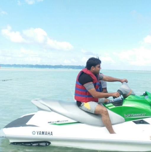
Amit Bansal
Work:
Axis Bank - Assistant Manager (2012)
Education:
Agra University - Bachelor of business Administration, Amity University - MBA
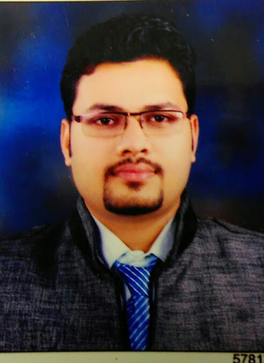
Amit Bansal
Work:
J.K. AGRAWAL & ASSOSIATES - CA ARTICLE (7)
Education:
CENTRA ACADEMY SEN. SEC. SCHOOL, DADABARI, KOTA - SCHOOLING
Tagline:
Awesome :))

Amit Bansal
Education:
Wright State University - Medicine, Loyola University Chicago - MA in Medical Sciences, Loyola University Chicago - BS in Biochemistry, Physics

Amit Bansal
Work:
IBM (India software labs) - Associate software engineer
Education:
KEC - Computer Science
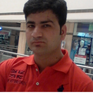
Amit Bansal
Work:
Addiraj dj eveant - Darecter (2012)
Education:
University of Delhi

Amit Bansal
Work:
Vinculum Solutions Ltd. - Project Manager (2007)
HCL Technologies - Lead Enginner (2003-2007)
HCL Technologies - Lead Enginner (2003-2007)
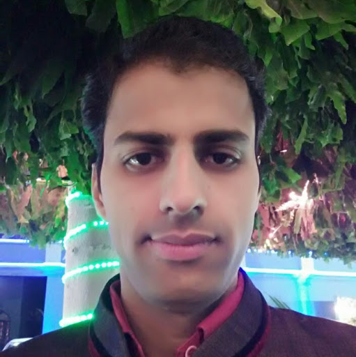
Amit Bansal
Work:
State Bank of India
Education:
Jiwaji University, Gwalior
Tagline:
"Winners do not do diffrent they do thing diffrently"
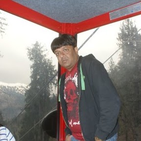
Amit Bansal
Work:
Bank Of Baroda - Senior Officer
Education:
Gaur Hari Singhania - MBA
Amit Kumar Bansal
view source
Amit Kumar Bansal
view source
Amit Bansal
view source
Amit Kumar Bansal
view source
Amit Kumar Bansal
view source
Amit Kumar Bansal
view source
Amit Shankar Bansal
view source
Amit Kumar Bansal
view sourceYoutube
Flickr
Get Report for Amit J Bansal from Jericho, NY, age ~50


